The prime has unveiled a new facility to support the development of microelectronic packaging technologies for defence applications.
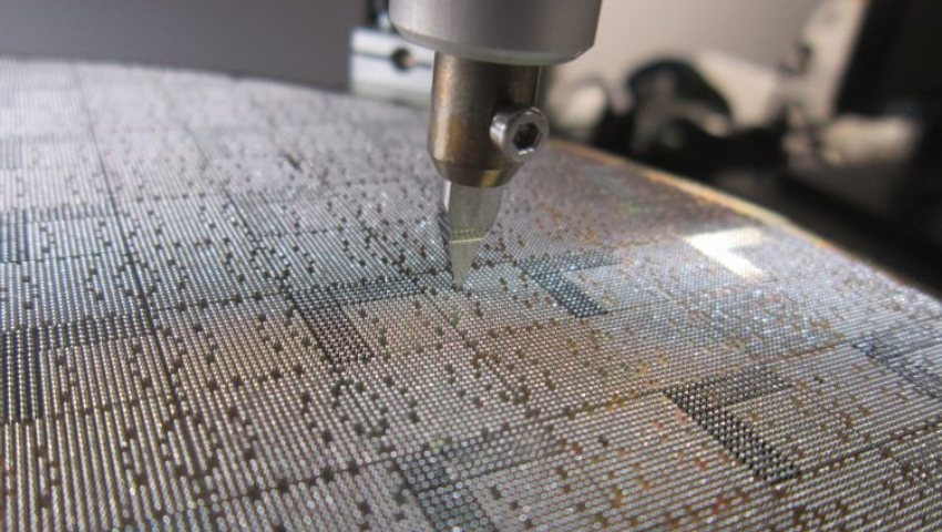
Northrop Grumman has opened its ‘Micro-Line’ (μ-Line) in Apopka, Florida, which establishes a wafer post-processing and test source tailored to support defence capability.
The μ-Line facility is expected to facilitate the development and production of critical microelectronics packaging technologies, with products processed at the μ-Line to support advanced radio frequency (RF) and electro-optic infrared (EO/IR) defence systems.
“The systems that Northrop Grumman builds need increasingly higher levels of device integration to meet customer performance, reliability and affordability requirements, no matter the domain and conditions where it will be used,” Scott Crudele, vice president of navigation targeting and survivability operations at Northrop Grumman, said.
“By establishing this new line we can provide our customers with a trusted packaging source to meet our quality specifications.”
The μ-Line is tipped to offer a complete suite of back-end wafer post-processing capabilities, including passivation, solder bumping, dicing, advanced inspection and test for up to 300mm wafers.
Semiconductors post-processed at the μ-Line will support both current and future Northrop Grumman programs.
The μ-Line packaging facility joins Northrop Grumman semiconductor foundries in Baltimore, Maryland, and Redondo Beach, California.
[Related: Northrop Grumman, Korean aerospace industry team up for JSTARS-K project]
Want to see more stories from trusted news sources?
Make Defence Connect a preferred news source on Google.
Click here to add Defence Connect as a preferred news source.
