The Pentagon’s DARPA has made a significant step forward in its Photonics in the Package for Extreme Scalability program, selecting teams of researchers to develop novel optical interconnect technologies. These are expected to vastly improve digital connectivity in microelectronics.
Advances in digital microelectronics have enabled indispensable capabilities for the US Department of Defense (DoD) in the fields of information processing, sensors and communications. Increasingly, system performance in these domains is constrained not by the limits of computation at individual chips, but rather by the electrical data movement between them. The energy efficiency and data bandwidth of electrical interconnects between integrated circuits (ICs) has failed to keep pace with improvements in transistor technology.
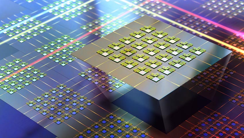
To address this challenge, DARPA developed the Photonics in the Package for Extreme Scalability (PIPES) program, which aims to expand the use of optical signaling for data transfer and place high-bandwidth photonics within the package of application-specific integrated circuits (ASICs) and field-programmable gate arrays (FPGAs). By targeting challenging goals for signaling efficiency and bandwidth density, PIPES seeks to enable disruptive system scalability and new system architectures capable of supporting emerging data-intensive applications for the commercial and defense industries.
Recently, DARPA selected teams to take on three research areas under PIPES. These efforts span the development and integration of the optical signaling technology for next-generation digital microelectronics, particularly targeting defence-relevant applications; the creation of component technologies and advanced link concepts to enable even greater technical performance; and the exploration of novel approaches to address the challenges and opportunities PIPES technologies present to system architects.
PIPES’ first research area is focused on the development of high-performance optical input/output (I/O) technologies packaged with advanced ICs, including FPGAs and ASICs. Two research teams led by Xilinx Corp and Intel will take on this research area. The resulting technologies will enable ICs with unprecedented bandwidth density, energy efficiency and reach. In addition, researchers from Lockheed Martin, Northrop Grumman, Raytheon and BAE Systems will help inform the development of these optical I/O technologies to ensure they address the requirements of current and future defence needs. The researchers will also investigate which defence applications could benefit most from this technology.
“The benefits of optical signaling in digital systems have been recognized for a long time,” said Dr Gordon Keeler, the DARPA program manager leading PIPES. “PIPES researchers are working to solve practical technical problems to meet the ambitious goals of the program, which include enabling I/O data rates up to 100 Terabits per second (Tbps) at signaling energies below one picoJoule per bit (pJ/bit). At the same time, the teams are studying how to tailor their technologies to address national security applications where operating conditions may be very demanding.”
The research teams selected to explore component technologies and advanced link concepts for novel approaches to in-package optical I/O include:
- Sandia National Laboratories
- University of California, San Diego
- University of California, Santa Barbara
- Columbia University
- The University of Pennsylvania
The final research area of the program is exploring system-level issues and opportunities created by high-performance optical I/O technologies for system architects. The University of California, Berkeley is taking on this research.
PIPES is part of the second phase of DARPA’s Electronics Resurgence Initiative (ERI) – a five-year, upwards of $1.5 billion investment in the future of domestic, US government and defence electronics systems. Under ERI Phase II, DARPA is working to ensure the development of novel manufacturing capabilities and to support a strategy for the enduring availability of differentiated, high-performance electronics for the DoD and its commercial partners.
Want to see more stories from trusted news sources?
Make Defence Connect a preferred news source on Google.
Click here to add Defence Connect as a preferred news source.